Voyager patent lays groundwork for space-grown crystals in optical communications

January 16, 2026
The materials that carry the world’s data, from fibre-optic cables to the chips inside hyperscale data centres, face natural limits in how precisely they can be made.
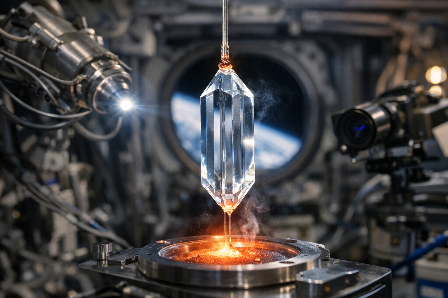
To date, manufacturing has always taken place under gravity, a condition that introduces tiny but consequential imperfections. Voyager Technologies believes producing these materials in space, without gravity, could result in far purer optical crystals, and has now secured a patent to do so in orbit.
The newly awarded patent covers an extraterrestrial manufacturing method that uses the microgravity environment of space to grow larger and more uniform crystals than is possible under Earth’s gravitational forces.
These crystals form the backbone of modern optical communications, enabling the transmission of light signals across data centres, fibre networks, and emerging space-based systems with minimal loss or distortion.
Why gravity limits optical crystal performance
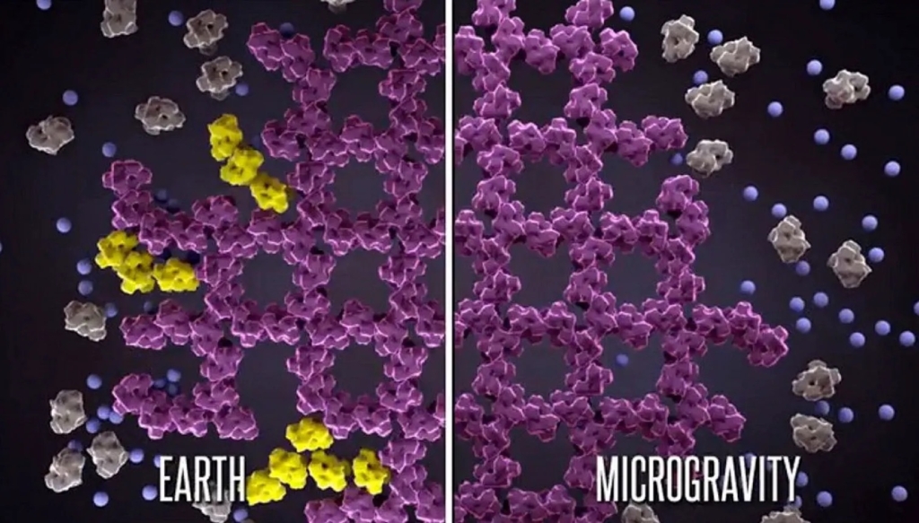
At the heart of the concept is a simple physical limitation. On Earth, gravity interferes with crystal growth. As crystals form, convection currents, sedimentation, and contact with container walls introduce defects at the atomic level.
Even microscopic imperfections can degrade performance when light is used to carry massive volumes of data, particularly at the speeds and bandwidths demanded by artificial intelligence workloads and cloud computing.
Microgravity changes that equation. In orbit, the absence of buoyancy-driven convection allows atoms to settle into more uniform structures, producing crystals with fewer defects and more consistent optical properties.
Voyager’s patented process is designed to take advantage of this environment by preventing crystal formation during ground handling, keeping all seed material in constant motion, and triggering growth only once the manufacturing payload reaches microgravity.
According to the company, the result is optical crystals that can be precisely tuned to a specific wavelength. By producing only the desired signal band and eliminating unintended spectral artefacts, the material could deliver cleaner transmission, higher signal stability, and lower error rates in high-bandwidth optical systems.
“Optical networks depend on fibres fabricated from crystal structures that are as perfect as materials science can make them,” said Dylan Taylor, chairman and chief executive of Voyager Technologies. “Ultra-pure, wavelength-engineered crystals are the foundation for faster, cleaner, and more resilient optical communications, whether in data centres on the ground or networks in orbit.”
How space manufacturing could reshape optical communications on Earth
While the manufacturing takes place in orbit, the intended impact is firmly terrestrial. High-performance optical materials underpin almost every part of the digital economy, from long-haul fibre networks and hyperscale data centres to advanced sensors and space communications terminals.
The patent reflects a growing interest across the space and materials science communities in using low Earth orbit not as an end market, but as a production environment.
Semiconductors, optical crystals, and other advanced materials are increasingly seen as high-value, low-mass products well suited to orbital manufacturing, where unique physical conditions can unlock performance gains that justify the cost of launch and return.
Voyager’s work parallels recent demonstrations in orbital semiconductor research, where microgravity has been shown to reduce defects in wide-bandgap materials used for power electronics, communications, and computing.
In both cases, the aim is not to replace Earth-based manufacturing but to enhance it by producing specialist materials or seed components in space that can then be scaled and integrated into existing terrestrial supply chains.
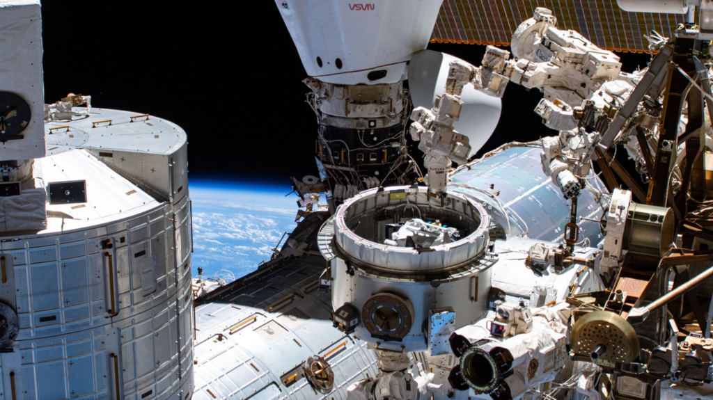
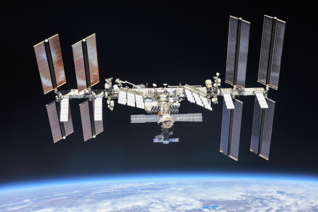
Testing orbital crystal manufacturing aboard the ISS
Voyager plans to validate its patented process with an in-orbit demonstration aboard the International Space Station in spring 2026.
The flight will be conducted under a grant through the ISS National Laboratory, allowing the company to observe crystal growth behaviour in long-duration microgravity and analyse the performance of returned samples.
The research effort brings together Voyager engineers with academic partners from the New Jersey Institute of Technology, New York University, and the Universities Space Research Association, reflecting the interdisciplinary nature of space-based materials development.
If successful, the experiment would mark another step towards routine orbital manufacturing of advanced optical materials, a field that until recently was largely confined to government-led research aboard crewed platforms.
Why microgravity enables purer optical crystal growth
The technical advantage of microgravity lies in its ability to suppress the physical processes that disrupt crystal formation on Earth.
Without gravity-driven flow, atoms arrange themselves more predictably. Without sedimentation, impurities are less likely to concentrate in specific regions. And without contact with container walls during growth, structural defects can be reduced.
For optical communications, these improvements translate directly into performance gains. Cleaner crystals mean lower signal attenuation, tighter wavelength control, and greater resilience under high data loads, all increasingly critical as networks strain to support AI training, cloud services, and real-time data processing.
As global demand for bandwidth continues to rise, the quality of the materials carrying that data is becoming as important as the electronics that drive the systems themselves.
The growing commercial case for orbital manufacturing
Voyager’s patent adds to a growing body of evidence that low Earth orbit may become an extension of advanced manufacturing rather than a niche research environment.
With launch costs falling and in-orbit operations becoming more routine, companies are increasingly exploring how space can be used to produce materials that are difficult or inefficient to make on Earth.
For optical communications, where performance margins are measured at the atomic scale, the appeal is clear. The challenge now lies in proving that orbital production can be reliably repeated, economically integrated, and safely scaled.
Voyager’s upcoming ISS experiment will be an early test of that proposition, and one that could help determine whether space-grown crystals move from laboratory curiosity to an enabling technology for the digital infrastructure that underpins modern life.